What Is the IRF7103TRPBF?
The IRF7103TRPBF is a dual N-channel power MOSFET housed in an SO-8 surface-mount package. It integrates two N-channel MOSFETs and has a drain-to-source voltage rating of 50V. Built on advanced HEXFET® planar technology, it significantly reduces on-resistance per unit area of silicon.
The device also features low gate charge and fast switching capability, with a maximum operating junction temperature of 150°C. The suffix "TRPBF" indicates tape-and-reel packaging for surface-mount assembly and compliance with RoHS lead-free requirements. It is commonly used in power management, load switching, and other power control circuits.
How Does the IRF7103TRPBF Work?
The IRF7103TRPBF operates using the electric-field control of N-channel enhancement-mode MOSFETs. It integrates two independent MOSFETs, each with a gate, source, and drain. When the gate-source voltage (VGS) exceeds the threshold voltage (typically 1.0–3.0 V), a conductive channel forms, allowing current to flow. When VGS falls below the threshold or reaches 0 V, the channel turns off, enabling fast switching.
Built on Infineon’s HEXFET® technology, the device offers low on-resistance (as low as 0.13 Ω at VGS = 10 V), reducing conduction losses. Its two independently controlled channels can operate as separate switches or be used in suitable power-control circuits. With PWM signals, it can help regulate power to motors and other loads.
Technical Specifications
This section lists the key specifications of the IRF7103TRPBF dual N-channel power MOSFET.
Parameter | Value |
Part Number | IRF7103TRPBF |
Manufacturer | Infineon Technologies |
Description | MOSFET 2N-CH 50V 3A 8-SOIC |
Lead Free Status / RoHS Status | Lead free / RoHS Compliant |
Rds On (Max) @ Id, Vgs | 130 mOhm @ 3A, 10V |
FET Feature | Standard |
FET Type | 2 N-Channel (Dual) |
Series | HEXFET® |
Drain to Source Voltage (Vdss) | 50V |
Gate Charge (Qg) (Max) @ Vgs | 30nC @ 10V |
Power - Max | 2W |
Vgs(th) (Max) @ Id | 3V @ 250µA |
Current - Continuous Drain (Id) @ 25°C | 3A |
Mounting Type | Surface Mount |
Input Capacitance (Ciss) (Max) @ Vds | 290pF @ 25V |
Packaging | Cut Tape (CT) |
Operating Temperature | -55°C ~ 150°C (TJ) |
Supplier Device Package | 8-SO |
Package / Case | 8-SOIC (0.154, 3.90mm Width) |
Base Part Number | IRF7103PBF |
Dual N-Channel Architecture Benefits
The IRF7103TRPBF integrates two independent N-channel MOSFETs in a single SO-8 surface-mount package, optimizing PCB space. Compared with using two separate single-channel MOSFETs, this design can reduce board space, simplify routing, and lower component count and BOM complexity.
The shared package supports compact thermal and electrical integration. Shorter current paths can help reduce parasitic inductance and resistance in high-frequency switching circuits, minimizing voltage spikes and improving signal integrity. The compact layout also allows for a more centralized thermal copper area, helping improve heat dissipation and system stability.
Pin Configuration
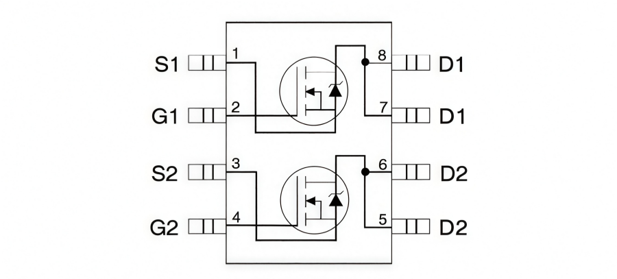
The IRF7103TRPBF comes in a standard 8-pin SO-8 package. Here are its pin descriptions listed:
The IRF7103TRPBF comes in a standard 8-pin SO-8 package. Here are its pin descriptions listed:
Pin 1 (S1): Source 1 – Current outlet/ground connection for Channel 1.
Pin 2 (G1): Gate 1 – Gate drive control signal input for Channel 1.
Pin 3 (S2): Source 2 – Current outlet/ground connection for Channel 2.
Pin 4 (G2): Gate 2 – Gate drive control signal input for Channel 2.
Pin 5 (D2): Drain 2 – Current inlet for Channel 2 (internally connected to Pin 6).
Pin 6 (D2): Drain 2 – Current inlet for Channel 2 (internally connected to Pin 5 for power dissipation and conduction).
Pin 7 (D1): Drain 1 – Current inlet for Channel 1 (internally connected to Pin 8).
Pin 8 (D1): Drain 1 – Current inlet for Channel 1 (internally connected to Pin 7 for power dissipation and conduction).
Power Dissipation and Thermal Management
The total power dissipation of the IRF7103TRPBF consists mainly of conduction losses (Pcond=I²RDS(on)) and switching losses at high frequencies. Due to its compact SO-8 package, heat must be dissipated primarily through the PCB pins and copper areas.
Key Thermal Parameters and Design Recommendations:
l Key Parameters: Junction-to-ambient thermal resistance (RθJA) ≈ 62.5°C/W, maximum junction temperature (Tj) = 150°C, and maximum power dissipation of approximately 2.0 W at an ambient temperature of 25°C.
l Drain Pin Copper Area: Use the internal drain connections at pins 5/6 (D2) and pins 7/8 (D1) to provide large 2 oz copper areas for heat dissipation.
l Thermal Vias and Derating: Add thermal vias beneath the pads to connect to internal or bottom-layer ground planes. At ambient temperatures above 50°C, derate the current as needed to keep the junction temperature below 120°C.
Gate Drive Requirements & Logic Compatibility
1. Drive Voltage vs. On-Resistance (VGS vs. RDS(on))
l Recommended Drive Voltage: A standard gate-drive voltage of 10 V provides low on-resistance (RDS(on) ≤ 0.13 Ω), minimizing conduction losses.
l Voltage Limits: The maximum gate-source voltage is ±20 V. A practical drive voltage of 10–15 V is recommended, subject to datasheet specifications.
2. Logic-Level Compatibility
l Threshold Voltage: The gate-source threshold voltage (VGS(th)) is 1.0–3.0 V.
l Direct MCU Drive Risks: Directly driving high-current loads from 3.3 V or 5 V MCU GPIO pins is not recommended, as the MOSFET may not turn on fully and could overheat.
l Design Recommendation: Use a gate driver IC or level-shifting circuit between the MCU and the gate to provide an appropriate drive voltage, such as 10 V.
3. Gate Drive Circuit Design
l Low Gate Charge: With a typical gate charge (Qg) of approximately 12 nC, the device can be suitable for high-frequency PWM switching, depending on the driver capability.
l Recommended Gate Resistor: A series gate resistor of 10–47 Ω can help suppress high-frequency oscillations.
l Gate Pull-Down Resistor: A 10 kΩ resistor between gate and source helps ensure reliable turn-off.
Peak Diode Recovery dv/dt Test Circuit
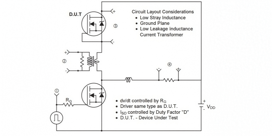
Typical Application Scenarios
The IRF7103TRPBF is suitable for space-constrained power switching and control circuits. Typical applications include:
DC-DC Converters
It is commonly used as a switching device in buck or boost converter designs when voltage, current, and switching requirements are met.
Power Management Circuits
The IRF7103TRPBF supports power switching and control in compact electronic systems.
Load Switching
It controls power delivery to electronic loads in embedded systems and consumer electronics.
Battery-Powered Devices
The MOSFET can be used in battery power switching and power-path control circuits within its electrical ratings.
Motor Control Circuits
The IRF7103TRPBF is suitable for switching small motor loads when the current, thermal limits, and drive requirements are properly managed.
SO-8 Package Outline
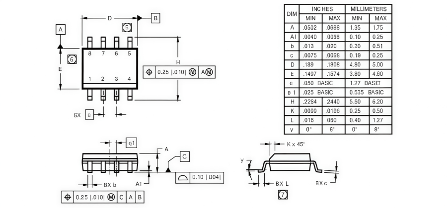
ANDE Electronics: Your Trusted Partner in Electronic Component Sourcing
At ANDE Electronics, we make getting the electronic components you need simple and fast. We work directly with top global manufacturers to provide high-quality components that have passed our strict checks, so you can count on them for your projects.
We also focus on quick and consistent delivery to keep your work on schedule and avoid delays. When you need reliable and efficient electronic parts for your projects, ANDE Electronics is a partner you can trust.