The BSS123-7-F is an N-channel enhancement-mode MOSFET housed in a compact SOT-23 package. It is suitable for applications such as small servo motor control, MOSFET gate driving, and low-current switching.
What Is BSS123-7-F?
The BSS123-7-F N-channel enhancement-mode FET manufactured by Diodes Incorporated using its proprietary high-density advanced trench technology.
In terms of key electrical specifications, the BSS123-7-F features a maximum drain-source voltage (VDS) of 100V, a continuous drain current (ID) of up to 170mA, and a gate-source voltage (VGS) of ±20V. Its maximum on-state resistance (RDS(on)) is approximately 6Ω at VGS = 10V, with an operating temperature range of -55°C to +150°C. It is suitable for electronic circuits where compact size and reliable switching control are required.
BSS123-7-F Specifications
This section lists the key specifications of the BSS123-7-F diode.
Parameter | Value |
Part Number | BSS123-7-F |
Manufacturer | Diodes Incorporated |
Input Capacitance (Ciss) (Max) @ Vds | 60pF @ 25V |
Drive Voltage (Max Rds On, Min Rds On) | 10V |
Lead Free Status / RoHS Status | Lead free / RoHS Compliant |
Packaging | Tape & Reel (TR) |
FET Type | N-Channel |
Technology | MOSFET (Metal Oxide) |
Rds On (Max) @ Id, Vgs | 6 Ohm @ 170mA, 10V |
Current - Continuous Drain (Id) @ 25°C | 170mA (Ta) |
Drain to Source Voltage (Vdss) | 100V |
Vgs (Max) | ±20V |
Mounting Type | Surface Mount |
Vgs(th) (Max) @ Id | 2V @ 1mA |
Power Dissipation (Max) | 300mW (Ta) |
Operating Temperature | -55°C ~ 150°C (TJ) |
Package | SOT-23-3 |
Base Part Number | BSS123 |
BSS123-7-F Pinout
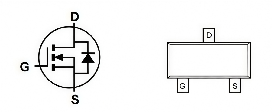
The BSS123-7-F is housed in a SOT-23 package with three pins: Drain (D), Gate (G), and Source (S). The functions of each pin are as follows:
l D (Drain): The drain pin connects to the load or drain-side circuit and carries the drain current.
l G (Gate): The gate pin controls the MOSFET's turn-on and turn-off by applying a gate-source voltage (VGS) to control the D-S channel.
l S (Source): The source pin provides the current return path and serves as the reference point for the gate-source voltage.
How Does BSS123-7-F Work?
The BSS123-7-F controls the conduction state between the Drain (D) and Source (S) through the voltage applied to the Gate (G). When VGS is below the gate threshold voltage, the D-S channel remains essentially off and the drain current is very small. When VGS exceeds the threshold, the electric field generated by the gate forms a conductive channel in the semiconductor, allowing current to flow from D to S.
With its low-level logic triggering characteristic, the BSS123-7-F can be driven by a high-level output from a microcontroller GPIO pin, allowing the transistor to turn on quickly. When the GPIO output goes low, the conductive channel disappears and the circuit switches off rapidly, enabling high-speed electronic switching control for small signals or low-power loads.
BSS123-7-F Features and Benefits
Here are the core features of BSS123-7-F below.
l Low Gate Threshold Voltage
l Low Input Capacitance
l Fast Switching Speed
l Low Input/Output Leakage
l High Drain-Source Voltage Rating
l Totally Lead-Free & Fully RoHS Compliant
l Halogen- and Antimony-Free. "Green" Device
l This part is qualified to JEDEC standards (as referenced in AEC-Q) for High Reliability.
l An automotive-compliant part is available under a separate datasheet (BSS123Q)
BSS123-7-F Applications
The BSS123-7-F is suitable for a variety of low-current switching and control circuits. Common applications include:
1. Small Servo Motor Controls
The BSS123-7-F can be used in small servo motor control circuits to quickly control the switching of motor-related loads through gate voltage, making it suitable for compact motor control systems.
2. Power MOSFET Gate Drivers
The device can be used in power MOSFET gate driver circuits to assist in driving power MOSFETs through fast switching control signals, making it suitable for power management and switching control circuits.
3. Switching Applications
With good switching response characteristics, the BSS123-7-F can be used as a low-current electronic switch for fast switching control of small loads, signals, or control lines.
4. Embedded Control Systems
Its compact SOT-23 package and low drive requirements make it suitable for embedded control circuits, where it can work with MCUs or logic controllers for load and signal control.
5. Industrial Control Circuits
The BSS123-7-F can be used for auxiliary switching, signal control, and low-power load switching in industrial control equipment, providing a simple switching solution for compact control circuits.
BSS123-7-F vs. BSS123
The BSS123-7-F and BSS123 have essentially the same core electrical performance. The main differences are in packaging and part-number suffixes.
l "-7" suffix: Indicates 7-inch Tape and Reel packaging for automated SMT assembly.
l "-F" suffix: Indicates a Lead-Free and RoHS-compliant version.
The BSS123-7-F is therefore a lead-free, tape-and-reel version of the BSS123, with the same basic function and application.
How to Test the BSS123-7-F?
Testing the BSS123-7-F, an N-channel MOSFET in a SOT-23 package, usually requires a multimeter in diode or resistance mode. Confirm the pinout before testing.
Step 1: Remove the Device
Desolder the BSS123-7-F from the circuit and place it on an insulated or ESD-safe surface. In-circuit testing may be affected by other components.
Step 2: Discharge the Device
Briefly short the G, D, and S pins with metal tweezers or a wire to discharge any residual charge.
Step 3: Test the Body Diode
Set the multimeter to diode mode. Connect the red probe to S and the black probe to D. A reading of about 0.4–0.9 V is expected. Reverse the probes; the meter should show OL.
Step 4: Turn the MOSFET On
Keep the black probe on S and briefly touch the red probe to G to charge the gate. Then move the red probe to D. The reading should drop significantly, close to 0 V, or the buzzer may sound, indicating that the channel is conducting.
Step 5: Turn the MOSFET Off
Keep the red probe on D and briefly touch the black probe to G to discharge the gate. Then move it back to S. The reading should return to the original 0.4–0.9 V body-diode reading or show OL, indicating that the channel is off.
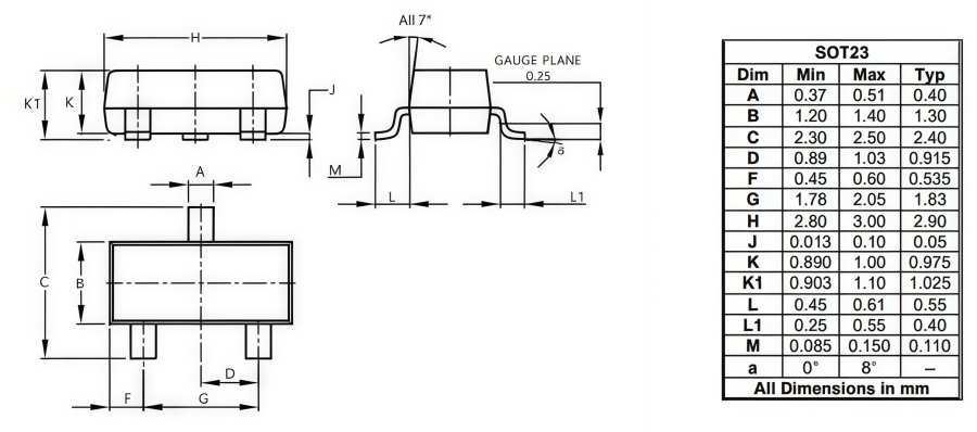
BSS123-7-F Package Outline Dimensions
ANDE Electronics: Your Trusted Partner in Electronic Component Sourcing
At ANDE Electronics, we make getting the electronic components you need simple and fast. We work directly with top global manufacturers to provide high-quality components that have passed our strict checks, so you can count on them for your projects.
We also focus on quick and consistent delivery to keep your work on schedule and avoid delays. When you need reliable and efficient electronic parts for your projects, ANDE Electronics is a partner you can trust.