What Is ATMEGA168PA-AU?
ATMEGA168PA-AU is a low-power CMOS 8-bit microcontroller based on the AVR enhanced RISC architecture and belongs to the ATmega168A/PA family. It features a reduced instruction set design that can execute many efficient instructions in a single clock cycle, making it suitable for a wide range of embedded applications.
In terms of processing performance, the architecture of the ATMEGA168PA-AU can achieve a throughput approaching 1 MIPS/MHz, allowing designers to balance processing speed and power consumption according to specific application requirements. Compared with traditional MCUs that may require multiple clock cycles to execute a single instruction, the efficient instruction execution of the AVR architecture helps improve system response while reducing unnecessary energy consumption.
ATMEGA168PA-AU Specifications
This section lists the key specifications of the ATMEGA168PA-AU under defined operating conditions.
Parameter | Value |
Part Number | ATMEGA168PA-AU |
Manufacturer | Microchip Technology |
Voltage - Supply (Vcc/Vdd) | 1.8 V ~ 5.5 V |
Data Converters | A/D 8x10b |
Lead Free Status / RoHS Status | Lead free / RoHS Compliant |
Operating Temperature | -40°C ~ 85°C (TA) |
Number of I/O | 23 |
Program Memory Size | 16KB (8K x 16) |
EEPROM Size | 512 x 8 |
Oscillator Type | Internal |
Series | AVR® ATmega |
RAM Size | 1K x 8 |
Program Memory Type | FLASH |
Speed | 20MHz |
Core Size | 8-Bit |
Connectivity | I²C, SPI, UART/USART |
Package | 32-TQFP (7x7) |
Base Part Number | ATMEGA168 |
ATMEGA168PA-AU Key Features
l High Performance, Low Power AVR® 8-Bit Microcontroller Family
l Advanced RISC Architecture
̶ 131 Powerful Instructions – Most Single Clock Cycle Execution
̶ 32 x 8 General Purpose Working Registers
̶ Fully Static Operation
̶ Up to 20 MIPS Throughput at 20MHz
̶ On-chip 2-cycle Multiplier
l High Endurance Non-volatile Memory Segments
̶ 4/8/16/32KBytes of In-System Self-Programmable Flash program memory
̶ 256/512/512/1KBytes EEPROM
̶ 512/1K/1K/2KBytes Internal SRAM
̶ Write/Erase Cycles: 10,000 Flash/100,000 EEPROM
̶ Data retention: 20 years at 85°C/100 years at 25°C(1)
̶ Optional Boot Code Section with Independent Lock Bits
l In-System Programming by On-chip Boot Program
l True Read-While-Write Operation
̶ Programming Lock for Software Security
l QTouch® library support
̶ Capacitive touch buttons, sliders and wheels
̶ QTouch and QMatrix™ acquisition
̶ Up to 64 sense channels
l Peripheral Features
̶ Two 8-bit Timer/Counters with Separate Prescaler and Compare Mode
̶ One 16-bit Timer/Counter with Separate Prescaler, Compare Mode, and Capture Mode
̶ Real Time Counter with Separate Oscillator
̶ Six PWM Channels
̶ 8-channel 10-bit ADC in TQFP and VQFN package
l Temperature Measurement
̶ 6-channel 10-bit ADC in SPDIP Package
l Temperature Measurement
̶ Programmable Serial USART
̶ Master/Slave SPI Serial Interface
̶ Byte-oriented 2-wire Serial Interface (Philips I2C compatible)
̶ Programmable Watchdog Timer with Separate On-chip Oscillator
̶ On-chip Analog Comparator
̶ Interrupt and Wake-up on Pin Change
l Special Microcontroller Features
̶ Power-on Reset and Programmable Brown-out Detection
̶ Internal Calibrated Oscillator
̶ External and Internal Interrupt Sources
̶ Six Sleep Modes: Idle, ADC Noise Reduction, Power-save, Power-down, Standby, and Extended Standby
ATMEGA168PA-AU Pin Configuration
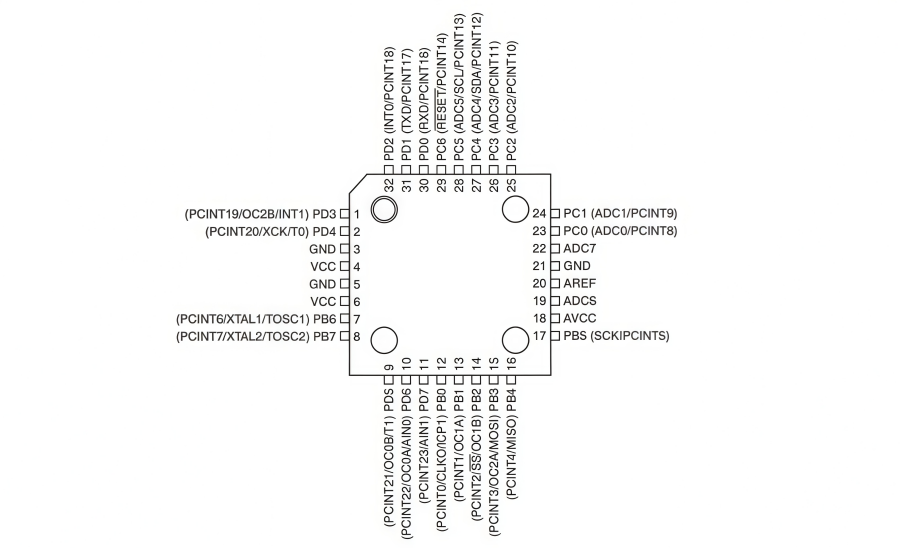
The ATMEGA168PA-AU 32-TQFP package features multifunctional pins that can be used for general-purpose I/O, external interrupts, USART, SPI, I2C, ADC, timers, and crystal oscillator connections. It also includes dedicated VCC, GND, AVCC, and AREF power and reference pins. The MCU pins are organized into three I/O port groups: PORTA, PORTB, and PORTD. The pins also support Pin Change Interrupt (PCINT) functions, providing flexible options for embedded peripheral expansion.
ATMEGA168PA-AU Functional Block Diagram
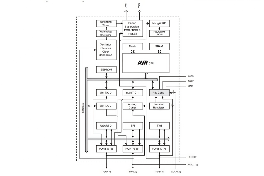
The ATMEGA168PA-AU adopts the AVR 8-bit RISC core. Its 32 general-purpose registers are directly linked to the ALU to perform dual-register operations in one clock cycle, outperforming traditional CISC microcontrollers in code efficiency. It integrates in-system-programmable Flash, EEPROM and SRAM, offering 23 GPIO lines, three Timer/Counters, multi-interrupt, USART, I²C, SPI interfaces, an 8-channel 10-bit ADC (TQFP package) and an internal watchdog oscillator.
It supports five software-configurable low-power modes: Idle, Power-down, Power-save, ADC Noise Reduction and Standby. The on-chip ISP Flash enables in-system programming and Read-While-Write for bootloader-based firmware updates. Supported by full development tools and the QTouch library, it fits diverse embedded control and capacitive-touch applications.
ATMEGA168PA-AU Programming and Development
ATMEGA168PA-AU supports In-System Programming (ISP), allowing developers to program and update the device through the SPI interface without removing the MCU from the target circuit board. Its AVR architecture is also supported by mature development tools and programming environments, making it suitable for embedded control, sensor, instrumentation, and other applications.
During development, designers can configure on-chip resources such as GPIO, ADC, timers, PWM, USART, SPI, and I2C/TWI according to project requirements, then use appropriate AVR development tools for code writing, compilation, programming, and debugging. Existing ATmega168PA-based designs can also take advantage of its range of peripheral interfaces to connect sensors, displays, and other external modules.
ATMEGA168PA-AU Application Fields
With its low-power AVR architecture, rich GPIO resources, and on-chip peripherals such as ADC, PWM, USART, SPI, and I2C/TWI, the ATMEGA168PA-AU can meet the needs of various embedded control and data processing applications, including:
1. Embedded Control Systems
The ATMEGA168PA-AU can be used in home appliances, control panels, and small automation devices. Its GPIO, timers, and PWM resources support functions such as button detection, status control, signal processing, and external device management.
2. Sensor Monitoring
With its 10-bit ADC and communication interfaces such as I2C/TWI and SPI, the MCU can connect to various sensors, including temperature, light, and pressure sensors, for analog or digital signal acquisition, conversion, and processing.
3. Industrial Instrumentation
The ATMEGA168PA-AU can be used in instrumentation and small industrial control systems. Its I/O, ADC, timers, and serial communication functions support device status monitoring, data acquisition, and basic control tasks.
4. Consumer Electronics
The MCU can be used in consumer electronics such as smart home appliances, electronic controllers, and portable devices. It provides reliable control and data communication for buttons, LEDs, display modules, and other peripheral components.
5. DIY and Embedded Projects
The ATMEGA168PA-AU is also suitable for electronic prototypes, educational experiments, and DIY embedded projects. Developers can flexibly connect sensors, displays, and other external modules according to their application requirements.
ATMEGA168PA-AU Package
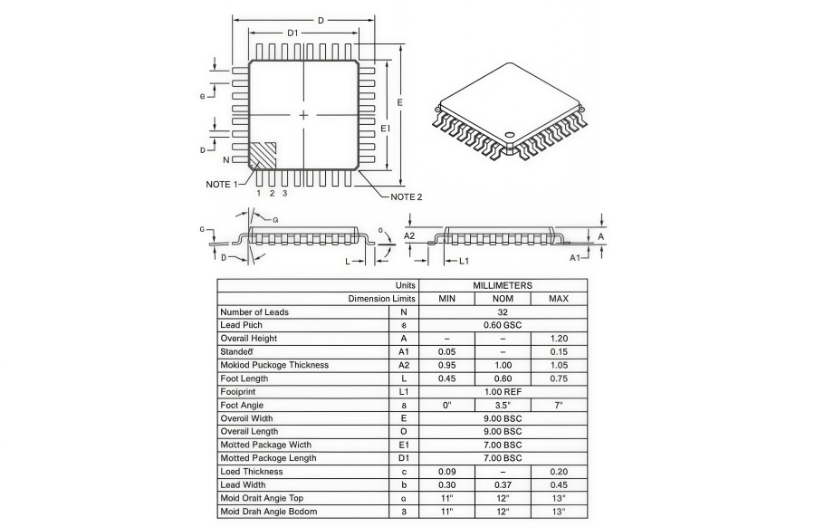
This part shows the package outlines of the ATMEGA168PA-AU microcontroller.
ANDE Electronics: Your Trusted Partner in Electronic Component Sourcing
At ANDE Electronics, we make getting the electronic components you need simple and fast. We work directly with top global manufacturers to provide high-quality components that have passed our strict checks, so you can count on them for your projects.
We also focus on quick and consistent delivery to keep your work on schedule and avoid delays. When you need reliable and efficient electronic parts for your projects, ANDE Electronics is a partner you can trust.