MX25L12835FMI-10G NOR Flash: Specs, Pinout & Applications
The MX25L12835FMI-10G is a 128Mb Serial NOR Flash memory from Macronix designed for high-speed code storage, firmware execution, and embedded boot applications. Supporting Standard SPI, Dual I/O, and Quad I/O interfaces, it combines fast data access, flexible erase/program operations, and long-term reliability, making it suitable for MCUs, MPUs, FPGAs, industrial controllers, networking equipment, and consumer electronics.
Memory Architecture: 128Mb (16MB) Serial NOR Flash organized for efficient page programming, with 256-byte pages and multiple erase options including 4KB sectors, 32KB/64KB blocks, and full-chip erase.
High-Speed Interface: Supports Standard SPI, Dual I/O, and Quad I/O read modes to accelerate firmware loading and system boot while reducing PCB complexity.
Reliability & Security: Delivers up to 100,000 program/erase cycles, integrated status registers, hardware/software protection mechanisms, and low standby power for reliable long-term data storage.
MX25L12835FMI-10G Core Specifications & Performance
Macronix MX25L12835FMI-10G technical specifications, attributes, parameters, and other vital data are below.
Parameter | Value |
Part Number | MX25L12835FMI-10G |
Manufacturer | Macronix |
Lead Free Status / RoHS Status | Lead free / RoHS Compliant |
Memory Type | Non-Volatile |
Technology | FLASH - NOR |
Memory Density | 128Mb (16MB) |
Memory Organization | 16M × 8 |
Interface | SPI, Dual SPI, Quad SPI (MXSMIO™) |
Supply Voltage (VCC) | 2.7 V ~ 3.6 V |
Page Size | 256 Bytes |
Sector Erase Size | 4 KB |
Block Erase Size | 32 KB / 64 KB |
Chip Erase | Supported |
Program/Erase Endurance | 100,000 cycles |
Clock Frequency | 104MHz |
Write Cycle Time - Word, Page | 30µs, 1.5ms |
Data Retention | Long-term non-volatile storage |
Power Modes | Active, Standby, Deep Power-Down |
Operating Temperature | -40°C ~ 85°C (TA) |
Supplier Device Package | 16-SOP |
Package | 16-SOIC |
Base Part Number | MX25L12835 |
Inside the Chip: MX25L12835FMI-10G Memory Architecture Explained
Below is an overview of the MX25L12835FMI-10G internal memory architecture and core operating mechanism.
1. Memory Array Organization
The MX25L12835FMI-10G provides 128Mb (16MB) of flash memory organized in a hierarchical structure:
l Page: 256 bytes, the minimum programming unit (65,536 pages).
l Sector: 4KB, the minimum erase unit (4,096 sectors).
l Block: 32KB or 64KB erase units (256 × 64KB blocks).
2. Interface and Transfer Modes
The device supports Standard SPI, Dual SPI, Quad SPI, and QPI (Quad Peripheral Interface).
l Single/Dual SPI: 1-bit or 2-bit data transfer.
l Quad SPI/QPI: 4-bit parallel transfer with up to 104MHz clock frequency and 416Mbps data throughput, supporting Execute-in-Place (XIP).
3. Core Hardware Modules
l X/Y Decoder: Selects the target memory cells.
l SRAM Buffer & State Machine: Buffers page data and controls programming/erase operations.
l HV Generator: Provides the high voltage required for programming and erase functions.
4. Data Protection Features
l Block Protect (BP Bits): Software-configurable write protection.
l WP# Pin: Hardware protection for the status register.
l 4K-bit OTP Area: One-Time Programmable memory for storing security keys or unique device IDs.
MX25L12835FMI-10G: Pin Configurations Listed

1. DNU/SIO3: Do not use in standard SPI mode; functions as SIO3 in Quad SPI mode.
2. VCC: 2.7–3.6 V power supply input.
3. RESET#: Active-low hardware reset input.
4. NC: No internal connection.
5. CS#: Active-low chip select signal.
6. SO/SIO1: Serial data output in SPI mode; SIO1 in Dual/Quad I/O mode.
7. WP#/SIO2: Active-low write protect input; SIO2 in Quad SPI mode.
8. GND: Ground reference.
9. SI/SIO0: Serial data input in SPI mode; SIO0 in Dual/Quad I/O mode.
10. SCLK: Serial clock input for SPI communication.
MX25L12835FMI-10G General and Software Features
GENERAL
l Supports Serial Peripheral Interface - Mode 0 and Mode 3
l Single Power Supply Operation
- 2.7 to 3.6 volts for read, erase, and program operations
l 134,217,728 x 1 bit structure or 67,108,864 x 2 bits(two /O mode) structure or 33,554,432 x 4 bits (four I/O mode) structure
l Protocol Support
- Single I/O, Dual I/O and Quad I/O
l Latch-up protected to 100mA from -1V to Vcc +1V
l Fast read for SPI mode
- Supports clock frequencies up to 133MHz for all protocols
- Supports Fast Read, 2READ, DREAD, 4READ, QREAD instructions.
- Configurable dummy cycle number for fast read operation
l Supports Performance Enhance Mode - XIP (execute-in-place)
l Quad Peripheral Interface (QPI) available
l Equal 4K-byte sectors, or Equal Blocks with 32K bytes or 64K bytes each
- Any Block can be erased individually
l Programming :
- 256-byte page buffer
- Quad Input/Output page program(4PP) to enhanceprogram performance
l Typical 100,000 erase/program cycles
l 20 years data retention
Software Features
l Input Data Format
- 1-byte Command code
l Advanced Security Features
- Block lock protection
The BP0-BP3 and T/B status bit defines the size of the area to be protected against program and erase
- Advanced sector protection function (Solid and Password Protect)
l Additional 4K bit secured OTP
- Features unique identifier
- Factory locked, identifiable, and customer lockable
l Command Reset
l Program/Erase Suspend and Resume operation
l Electronic Identification
- JEDEC 1-byte manufacturer ID and 2-byte device ID
- RES command for 1-byte Device ID
- REMS command for 1-byte manufacturer ID and 1-byte device ID
l Supports Serial Flash Discoverable Parameters(SFDP) mode
MX25L12835FMI-10G Functional Block Diagram
The block diagram illustrates the internal architecture and data flow of the MX25L12835 flash memory. External commands, addresses, and data are received through the I/O interface pins (SI/SIO0, SO/SIO1, SIO2, SIO3, CS#, WP#, and HOLD#/RESET#). Driven by the Clock Generator, commands are decoded by the Mode Logic and State Machine, while addresses are routed through the Address Generator to the X-Decoder and Y-Decoder for memory access.
During programming and erase operations, data is buffered in the Data Register and SRAM Buffer, with high voltage supplied by the HV Generator. During read operations, stored data is amplified by the Sense Amplifier and transmitted through the Output Buffer to the I/O pins.
 a
a
Typical Applications of MX25L12835FMI-10G Memory
The MX25L12835FMI-10G features high-capacity storage, a high-speed SPI interface, low power consumption, and reliable data protection, making it well suited for program and data storage in a wide range of embedded systems.
1. Industrial Control Systems
The MX25L12835FMI-10G is widely used as program memory in industrial control equipment to store firmware, configuration parameters, and operational data. Its high-speed read performance and reliable data retention help improve system startup speed and overall stability.
2. Consumer Electronics
This flash memory is commonly used in consumer electronics to store boot code, operating systems, application software, and user configuration data, enabling fast boot times and reliable system operation.
3. Networking and Communication Equipment
With its high-speed Quad SPI interface and Execute-in-Place (XIP) capability, the MX25L12835FMI-10G is well suited for networking and communication devices that require fast code execution and firmware storage, improving overall system responsiveness.
4. Automotive Electronics
The MX25L12835FMI-10G can be used in automotive electronic control units (ECUs) and infotainment systems to store boot code, configuration files, and firmware, providing reliable non-volatile memory for automotive applications.
5. Internet of Things (IoT) Devices
In IoT applications, the device stores MCU firmware, wireless protocol stacks, and configuration data. It also supports over-the-air (OTA) updates and long-term reliable operation for low-power embedded systems.
6. Medical and Smart Instruments
The MX25L12835FMI-10G serves as program and data memory in medical equipment and smart instruments, ensuring stable operation while securely storing critical parameters and historical data.
Common Design Challenges of MX25L12835FMI-10G NOR Flash
When designing with the MX25L12835FMI-10G, maintaining signal integrity and power stability is essential, especially during high-speed SPI communication and program/erase operations. Proper PCB layout, short SPI traces, a solid ground plane, and adequate decoupling capacitors help ensure reliable performance and minimize communication errors.
Another important consideration is flash memory management. Since data must be erased before being rewritten, developers should optimize sector erase operations and configure write protection features correctly to prevent accidental data modification. For systems that support firmware updates, implementing backup or recovery mechanisms can further improve reliability and ensure safe boot operation.
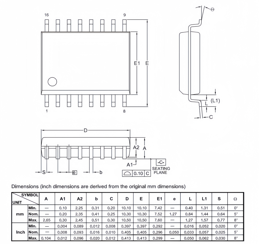
MX25L12835FMI-10G Package Outline
This section presents the physical package specifications and pin dimensions of the MX25L12835FMI-10G flash memory.
ANDE Electronics: Your Trusted Partner in Electronic Component Sourcing
At ANDE Electronics, we make getting the electronic components you need simple and fast. We work directly with top global manufacturers to provide high-quality components that have passed our strict checks, so you can count on them for your projects.
We also focus on quick and consistent delivery to keep your work on schedule and avoid delays. When you need reliable and efficient electronic parts for your projects, ANDE Electronics is a partner you can trust.