LE55PQW-HSB1 Description
The LE55PQW is a 55-inch color active matrix OLED display panel that uses Oxide Thin Film Transistor (Oxide TFT) technology as the active element. It adopts a bottom-emission OLED structure and features a QWUXGA resolution of 3840 × 2160 pixels, delivering detailed image quality for large-screen display applications.
The LE55PQW-HSB1 uses an RWBG vertical stripe pixel structure, where each pixel consists of Red, Green, Blue, and White sub-pixels. With a 10-bit grayscale signal for each sub-pixel, the panel can reproduce more than 1.07 billion true colors, providing smooth color transitions and high color accuracy. Itis designed for applications requiring high brightness, ultra-wide viewing angles, wide color gamut, high color depth, and fast response performance, such as premium TVs and large-format display systems.
LE55PQW-HSB1 General Specifications
The following table provides an overview of the key specifications of the LE55PQW-HSB1 LCD display module.
Parameter | Specification |
Model | LE55PQW-HSB1 |
Brand | |
Display Size | 55" |
Composition | OLED Display Module |
Resolution | 3840(H) × 2160(V), QWUXGA |
Luminance | 550 cd/m² (Typ.) |
Contrast Ratio | 200,000:1 (Typ.) |
Viewing Angle | 120/120/120/120 (Min.) |
View Direction | Symmetry |
Color Depth | 10-bit, 1.07 Billion Colors |
Pixel Format | RWBG Vertical Stripe |
Display Mode | Normally Black |
Surface Treatment | Hard Coating (2H), Anti-Reflection |
Active Area | 1221.4(H) × 695.7(V) mm |
Outline Size | 1221.4(H) × 695.7(V) × 0.79(D) mm |
Response Time | 0.1 ms (Typ.) G-to-G |
Refresh Rate | 120Hz (Typ.) |
Interface Type | V-by-One HS, 16 Lane |
Touch Screen | Without |
Light Source | OLED (Self Emissive) |
Power Supply | VDD 12V / EVDD 22V |
Power Consumption | 110.3W (Typ.) |
Weight | 2.1kg (Typ.) |
Operating Temperature | 0 ~ 45°C |
Storage Temperature | -20 ~ 60°C |
LE55PQW-HSB1 Display Signal Path Explained
Main Controller → Interface → LCD Driver → TFT Panel → Backlight
The display signal transmission process is the core workflow that enables an LCD module to generate images. First, the Main Controller generates image data, including RGB color information, synchronization signals, and control commands. The data is then transmitted to the LCD module through the Interface. Common interfaces include LVDS, RGB, and MIPI, which provide high-speed and stable data communication while reducing signal interference during transmission.
After receiving the image signals, the LCD Driver processes and converts the data into control voltages required by the TFT panel, driving the switching states of each TFT pixel unit. By adjusting the light transmission of RGB sub-pixels, the TFT Panel produces images with different brightness levels and colors. Meanwhile, the Backlight provides uniform illumination for transmissive LCDs, allowing the light modulated by the liquid crystal layer to be visible and delivering a complete, clear display output.
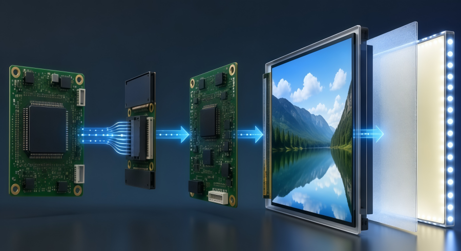
LE55PQW-HSB1 Hardware Interface and Driver Circuit Design
In the hardware design of the LE55PQW-HSB1 OLED module, accurate interface matching and timing control are essential for stable display performance.
1. Signal Interface and Timing Control
The LE55PQW-HSB1 uses a high-bandwidth V-by-One interface for high-resolution image transmission. Hardware design requires proper impedance matching and equal-length routing for differential signals (RxIN±) and clock lines (RxCLK±) to reduce signal loss and interference. JEIDA/VESA format configuration and display timing signals, including HS/VS synchronization and DE timing, must be correctly matched to ensure stable pixel clock operation and prevent image artifacts or flickering.
2. Backlight Driver Circuit and Control
The module’s WLED backlight requires an external LED constant-current driver board (typically powered by 24V DC) with stable power output. The main board controls backlight activation through the BL_ON signal, while 100Hz–1kHz PWM dimming can be used for brightness adjustment. Protection features such as over-voltage, over-current protection, and soft-start are recommended to prevent damage caused by surge current.
3. Power On/Off Sequence Control
To ensure reliable operation and prevent display issues, the LE55PQW-HSB1 requires a proper power sequence. During startup, the logic power (VDD) should be enabled first, followed by image data input (LVDS/V-by-One), and then the BL_ON signal to activate the backlight. During shutdown, the backlight should be turned off first, followed by stopping image data transmission and finally disabling the logic power. This sequence helps maintain stable image switching and extends panel lifetime.
LE55PQW-HSB1 Large Screen Advantages and Benefits
The LE55PQW-HSB1 OLED delivers excellent color performance, providing a clear and realistic visual experience for large-screen display applications.
l 55-inch large-screen OLED display design, providing a wider and more immersive viewing experience.
l Uses oxide TFT active matrix technology, improving pixel control accuracy and display stability.
l Supports QWUXGA 3840×2160 resolution, delivering detailed and clear 4K image quality.
l Adopts RWBG (Red, Green, Blue, White) sub-pixel structure, enhancing color reproduction performance.
l Supports 10-bit grayscale control, enabling smoother brightness transitions.
l Displays more than 1.07 billion true colors, providing richer color levels and more accurate image details.
l Supports 10-bit 16-lane V-by-One Interface, meeting high-speed image transmission requirements.
l Provides high brightness performance, making it suitable for large-screen visual applications.
LE55PQW-HSB1 Functional Block Diagram
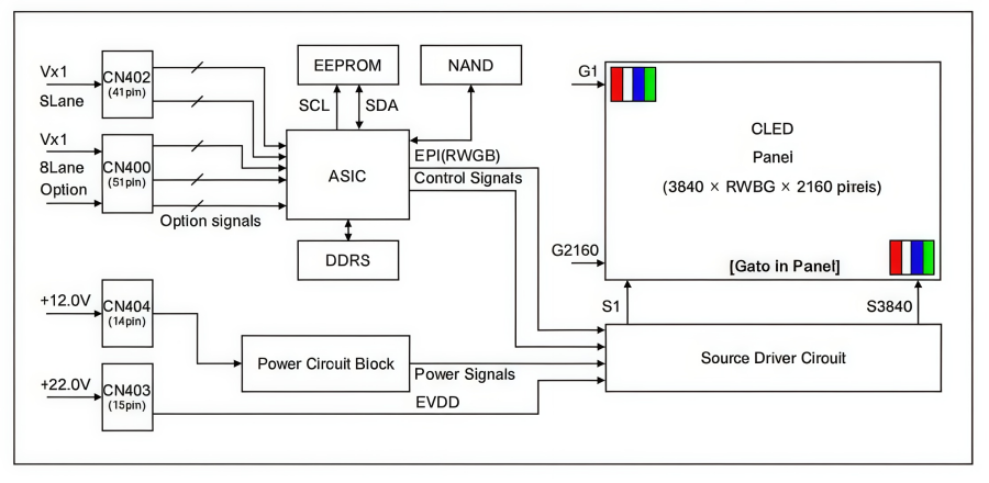
The LE55PQW OLED display system mainly consists of three parts: signal processing, power management, and pixel driving.
External 8-Lane V-by-One (Vx1) image signals and control signals are input to the ASIC main controller through CN402 and CN400. The ASIC processes image data and works with EEPROM, NAND Flash, and DDR3 for EDID parameter reading, compensation data storage, and image buffering. The processed data is transmitted to the Source Driver through the EPI protocol, while the GIP circuit is controlled to complete panel scanning.
For power management, the +12V main power input from CN404 is converted by the Power Circuit into different voltages required by the system. The +22V EVDD power input from CN403 directly supplies the Source Driver for OLED pixel driving. Finally, the Source Driver outputs S1~S3840 drive signals to precisely control the 3840×RWBG×2160 4K OLED panel, delivering high-quality image performance.
LE55PQW-HSB1 for Large Display Applications
The LE55PQW-HSB1 is designed for large-screen display applications that require excellent image quality, wide viewing angles, and smooth dynamic performance. It is especially suitable for premium TVs and professional audiovisual display systems.
1. Premium Smart TV
The LE55PQW-HSB1 can serve as a core display panel for high-end smart TVs. With OLED self-emissive technology, it delivers an immersive viewing experience for home entertainment systems.
l 4K OLED smart TVs
l High-end home theater TVs
l Large-screen audiovisual entertainment displays
2. Home Theater Display
For home theater applications, the LE55PQW-HSB1 provides an excellent viewing experience with its ultra-wide viewing angle, high color gamut, and high color depth, meeting the requirements of movies, HDR videos, and premium content playback.
l OLED home theater displays
l HDR audiovisual systems
l Premium private cinema equipment
3. Gaming TV & Display
The LE55PQW-HSB1 supports fast response performance and high-quality image output, helping reduce motion blur and display delays. It is suitable for gaming applications that require smooth and responsive visuals.
l Large-size OLED gaming TVs
l Console gaming displays
l Gaming entertainment terminals
4. Commercial Large Displays
With its large display area and excellent color performance, the LE55PQW-HSB1 is suitable for commercial display applications, providing clear presentation of advertising content and dynamic visuals.
l Shopping mall display TVs
l Brand promotional screens
l Commercial audiovisual display terminals
Operating Precautions
1) Avoid spike noise, as it may cause circuit malfunction. The over/under shoot voltage should be controlled within ±200mV.
2) Response time varies with temperature and becomes longer under low-temperature conditions.
3) Prevent condensation during sudden temperature changes, as moisture may damage the polarizer and electrical contacts, causing display defects.
4) Avoid displaying fixed patterns for long periods, as image retention may occur. Use screen protection or brightness reduction functions when necessary.
5) Reduce electromagnetic interference (EMI) through proper grounding and shielding due to high-frequency circuits inside the module.
6) Avoid mechanical or acoustic impacts to ensure the module maintains normal operating performance.
7) Use proper machine screws for fixation to prevent conductive particles from damaging the module.
8) Do not place the OLED module on its edge during handling or installation.
9) Keep Wi-Fi antennas away from the source PCB and FFC area to prevent signal noise interference.
ANDE Electronics: Reliable LCD Display Solutions
As a professional display supplier, Ande Electronics is committed to providing LCD modules that meet modern application needs.
We offer not only high-quality display products but also reliable technical support and flexible purchasing options. Our experienced engineering team works closely with customers to provide guidance on module selection, integration, and optimization.
Choosing Ande Electronics, then engineers and manufacturers will gain a partner focused on quality, innovation, and efficiency.