AT89S8253-24AU Overview
The AT89S8253-24AU is a CMOS 8-bit microcontroller with 12KB In-System Programmable (ISP) Flash program memory and 2KB EEPROM data memory. It is built using high-density non-volatile memory technology and is compatible with the industry-standard MCS-51 instruction set and pin configuration. The on-chip downloadable Flash allows the program memory to be reprogrammed in-system through an SPI serial interface or a conventional non-volatile memory programmer.
This microcontroller features 256 bytes of RAM, 32 programmable I/O lines, a watchdog timer, two data pointers, three 16-bit timers/counters, and a six-vector, four-level interrupt system. It uses static logic, allowing operation at zero frequency, and supports two power-saving modes: Idle Mode, which stops the CPU but keeps RAM, timers, serial port, and interrupts running; and Power-down Mode, which preserves RAM and freezes the oscillator until the next interrupt or reset.
For programming, the on-chip Flash/EEPROM can be accessed via the SPI serial interface. When the RESET signal is held active, the SPI bus enters the serial programming mode, allowing the program memory to be read or written, unless one or more lock bits are set.
AT89S8253-24AU Key Specs
Parameter | Value |
Part Number | AT89S8253-24AU |
Description | IC MCU 8BIT 12KB FLASH 44TQFP |
Lead Free Status / RoHS Status | Lead free / RoHS Compliant |
Voltage - Supply (Vcc/Vdd) | 2.7 V ~ 5.5 V |
Operating Temperature | -40°C ~ 85°C (TA) |
Base Part Number | AT89S8253 |
Core Size | 8-Bit |
Connectivity | SPI, UART/USART |
Series | 89S |
Package | 44-TQFP (10x10) |
EEPROM Size | 2K x 8 |
Oscillator Type | External |
Number of I/O | 32 |
RAM Size | 256 x 8 |
Speed | 24MHz |
Core Processor | 8051 |
Peripherals | POR, WDT |
Packaging | Tray |
Moisture Sensitivity Level (MSL) | 3 (168 Hours) |
Program Memory Type | FLASH |
Program Memory Size | 12KB (12K x 8) |
AT89S8253-24AU Pinout

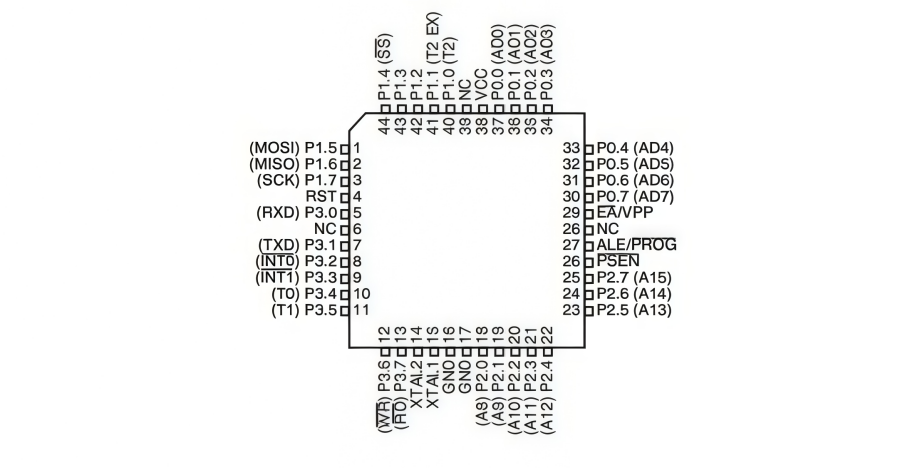
The AT89S8253-24AU comes in a 44-TQFP, with pin functions compatible with the standard MCS-51 microcontroller series. It features four 8-bit I/O ports (P0–P3), each usable for general-purpose input/output. The P0 port can serve as a multiplexed low-order address/data bus, while the P2 port provides high-order address output. The pins also include RST (reset), XTAL1/XTAL2 (crystal oscillator inputs), and special function pins for external interrupts and timer control, such as INT0/INT1 and T0/T1.
In addition, the AT89S8253-24AU provides SPI interface pins (MOSI, MISO, SCK) to support in-system serial programming of the on-chip Flash. Other key control pins, such as EA/VPP, ALE/PROG, and PSEN, are used for program memory access selection, address latching, and external program reading, allowing flexible system design and enabling a variety of embedded control and peripheral expansion applications.
AT89S8253-24AU Technical Features
• Compatible with MCS®51 Products
• 12K Bytes of In-System Programmable (ISP) Flash Program Memory
– SPI Serial Interface for Program Downloading
– Endurance: 10,000 Write/Erase Cycles
• 2K Bytes EEPROM Data Memory
– Endurance: 100,000 Write/Erase Cycles
• 64-byte User Signature Array
• 2.7V to 5.5V Operating Range
• Fully Static Operation: 0 Hz to 24 MHz (in x1 and x2 Modes)
• Three-level Program Memory Lock
• 256 x 8-bit Internal RAM
• 32 Programmable I/O Lines
• Three 16-bit Timer/Counters
• Nine Interrupt Sources
• Enhanced UART Serial Port with Framing Error Detection and Automatic
Address Recognition
• Enhanced SPI (Double Write/Read Buffered) Serial Interface
• Low-power Idle and Power-down Modes
• Interrupt Recovery from Power-down Mode
• Programmable Watchdog Timer
• Dual Data Pointer
• Power-off Flag
• Flexible ISP Programming (Byte and Page Modes)
– Page Mode: 64 Bytes/Page for Code Memory, 32 Bytes/Page for Data Memory
• Four-level Enhanced Interrupt Controller
• Programmable and Fuseable x2 Clock Option
• Internal Power-on Reset
• 42-pin PDIP Package Option for Reduced EMC Emission
• Green (Pb/Halide-free) Packaging Option
AT89S8253-24AU Block Diagram

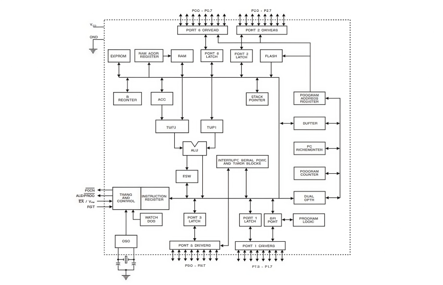
The internal architecture (Block Diagram) of the AT89S8253 illustrates a typical 8051 core layout. From the logic block diagram, it can be seen that the chip integrates a high-performance ALU (Arithmetic Logic Unit) and multiple memory modules, including RAM for data buffering, FLASH for program code storage, and EEPROM for non-volatile data storage. Additionally, the architecture features an instruction register, a Stack Pointer, and a Program Counter, which, together with the Timing and Control unit, ensure efficient instruction decoding and execution.
For external interaction and expandability, the architecture provides four 8-bit parallel interfaces (Port 0–3), each equipped with corresponding drivers and latches, supporting general-purpose I/O operations. To enhance communication and system reliability, the chip also integrates an SPI serial communication module, an interrupt system, and a Watchdog Timer, which effectively prevents program runaway and supports multi-device networking. At the bottom, the oscillator circuit (OSC) connects to an external crystal, providing precise clock timing for the entire MCU system.
AT89S8253-24AU Applications
1. Industrial Control Systems
The AT89S8253-24AU can serve as the core MCU in industrial automation controllers, used for collecting sensor data, executing control algorithms, and driving actuators. It performs excellently in PLCs (Programmable Logic Controllers), temperature control systems, and automated production lines.
2. Smart Home Devices
This MCU supports multiple communication interfaces and an interrupt system, making it suitable for integration into smart home devices for functions such as lighting control, automated curtains, or security monitoring. Its EEPROM can store user settings, enabling state recovery after power loss.
3. Data Acquisition and Measurement Instruments
With high-speed internal RAM and FLASH, the AT89S8253-24AU can collect and process various sensor data, such as temperature, humidity, and pressure, making it suitable for portable or laboratory measurement instruments.
4. Consumer Electronics
The MCU is compact and low-power, making it ideal as the control core for consumer electronics such as electronic toys, portable devices, and small home appliances. It can drive motors and buzzers via I/O interfaces to implement complex logic control and user interactions.
5. Communication and Networking Devices
The AT89S8253-24AU integrates an SPI serial port, suitable for simple communication interfaces and network devices, enabling data transfer, protocol processing, and multi-device networking control.
6. Safety and Protection Systems
With an integrated Watchdog Timer and interrupt system, the MCU is suitable for safety alarms and protection systems, ensuring reliable operation under abnormal conditions.
ANDE Electronics: Your Trusted Partner in Electronic Component Sourcing

At ANDE Electronics, we make getting the electronic components you need simple and fast. We work directly with top global manufacturers to provide high-quality components that have passed our strict checks, so you can count on them for your projects.
We also focus on quick and consistent delivery to keep your work on schedule and avoid delays. When you need reliable and efficient electronic parts for your projects, ANDE Electronics is a partner you can trust.


