RT9059GSP Overview
The RT9059GSP is a high-performance positive linear voltage regulator, typically used in applications requiring very low input voltage and low dropout voltage, capable of delivering up to 3A of output current. It operates with an input voltage as low as 1V and a 3V VDD, and its output voltage can be programmed down to 0.8V, making it ideal for scenarios where VOUT is very close to VIN.
The device features an integrated Enable pin, which further reduces power consumption during shutdown while maintaining stable output voltage regulation to handle variations in line, load, and temperature. The RT9059GSP also provides a Power-Good signal to indicate when the output voltage reaches 90% of its rated value. Its recommended junction temperature range is −40°C to 125°C, and the ambient temperature range is −40°C to 85°C, supporting operation across a wide temperature range.
RT9059GSP Key Specs
Parameter | Value |
Part Number | RT9059GSP |
Description | IC REG LINEAR 3A 8SOP |
Lead Free Status / RoHS Status | Lead free / RoHS Compliant |
Control Features | Enable |
Voltage - Input (Max) | 5.5V |
Moisture Sensitivity Level (MSL) | 3 (168 Hours) |
Voltage Dropout (Max) | 0.45V @ 3A |
Current - Output | 3A |
Operating Temperature | -40°C ~ 85°C (TA) |
Voltage - Output (Min/Fixed) | 3V |
Output Configuration | Positive |
Voltage - Output (Max) | 5.5V |
Supplier Device Package | 8-SOP-EP |
Manufacturer Standard Lead Time | 16 Weeks |
Packaging | Tape & Reel (TR) |
Number of Regulators | 1 |
Current - Quiescent (Iq) | 1.2mA |
Package / Case | 8-SOIC (0.154, 3.90mm Width) Exposed Pad |
Protection Features | Over Current, Over Temperature |
RT9059GSP Pin Description

1. PG
Power-good indicator. This open-drain output pin is pulled high when the VOUT or FB voltage is within the target range. It is pulled to ground under protection conditions, EN shutdown, or during the soft-start period.
2. EN
Enable control input. A logic-high enables the converter, while a logic-low forces the device into shutdown mode. Connect this pin to the VIN pin to conserve the system’s power rail, or connect this pin to an external power rail for power sequence control. It is recommended to apply the enable voltage after the VIN pin voltage is ready for the correct soft-start function. Do not leave this pin floating.
3. VIN
Supply voltage input. The input voltage range is from 1V to 5.5V. A suitable input capacitor should be placed close to this pin to minimize voltage spikes and noise, ensuring a stable input voltage.
4. VDD
Supply voltage of the control circuit. This pin provides the necessary power for the internal control logic and analog circuitry. It is important to ensure that the VDD voltage is stable and within the specified range to guarantee proper operation of the device.
5. NC
No internal connection. Connect this pin to the GND plane of the top layer to extend the GND copper area to enhance the thermal performance.
6. VOUT
LDO output pin. Connect a ceramic capacitor with a capacitance of at least 10F as close as possible from this pin to GND to minimize the output impedance.
7. ADJ
Feedback voltage input. This pin is used to set the output voltage via an external resistive voltage divider. The feedback reference voltage is 0.8V (typical). Place the resistive voltage divider as close to the FB pin as possible. Do not leave this pin floating.
8. GND
GND Ground. The exposed pad must be soldered to a large PCB and connected to GND for maximum power dissipation.
RT9059GSP Simplified Application Circuit

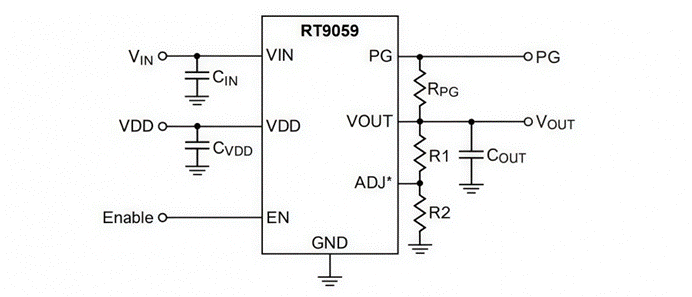
This circuit shows a typical application of the RT9059GSP. VIN is the input voltage pin. The input capacitor CIN filters the voltage to ensure a stable input. VDD powers the internal circuits and is also connected to a filter capacitor CVDD to keep the regulator stable. EN is the enable pin, used to turn the device on or off. When EN is high, the regulator works; when EN is low, it enters low-power shutdown. GND is the ground pin and provides a common reference for the circuit.
The output voltage comes from the VOUT pin. External resistors R1 and R2 set the adjustable output, with the ADJ pin used for voltage division. COUT filters the output to reduce voltage ripple and improve regulation accuracy. PG is the power-good signal pin. Through the pull-up resistor RPG, PG goes high when VOUT reaches 90% of its rated value, indicating that the system power is normal. The overall circuit is simple and efficient, suitable for applications requiring low dropout and high-precision voltage regulation.
RT9059GSP Features
l Output Current up to 3A
l High Accuracy ADJ Voltage (1.5%)
l Dropout Voltage: 350mV @ 3A (Typical)
l Wide Input Voltage Range: 1V to 6V
l Programmable Output Voltage: 0.8V and above
l VOUT Power-Good Signal
l VOUT Pull Low Resistance when Disabled
l Current-Limit Protection
l Over‐Temperature Protection
l Fast Transient Response
l Low Quiescent Current
l Stable with Ceramic Capacitors
l Low Output Noise
RT9059GSP Applications
Notebook PC
The RT9059GSP provides high-accuracy core voltage regulation for notebook computers. It supports low input voltage and up to 3A output current, meeting the transient load needs of CPUs, GPUs, and other core chips. Its low dropout and low-noise output help extend battery life and improve overall power efficiency.
Motherboard Applications
On motherboards, the RT9059GSP can regulate voltage for processors, memory, or chipsets. It keeps the system stable under high load or temperature changes. Built-in overcurrent and thermal protection prevent damage, and the adjustable output adds flexibility for motherboard power design.
Graphics Cards / GPU Voltage Regulation
GPUs need precise voltage and fast response. The RT9059GSP delivers stable core voltage with fast transient response. It reduces performance fluctuations and power waste. Even under heavy load, it maintains low dropout and low noise, improving GPU stability and performance.
Industrial Control Boards
Industrial control boards require reliable and noise-resistant power. The RT9059GSP offers high-accuracy regulation, low output noise, and multiple protections. It is suitable for PLCs, servo controllers, and sensor interface power supplies, providing stable voltage to critical chips.
Networking Equipment (Routers, Switches)
In routers and switches, the RT9059GSP supplies low-noise, high-accuracy voltage to processors, network interface chips, and high-speed modules. Its low dropout and adjustable output help reduce power consumption and improve energy efficiency.
RT9059GSP Functional Block Diagram

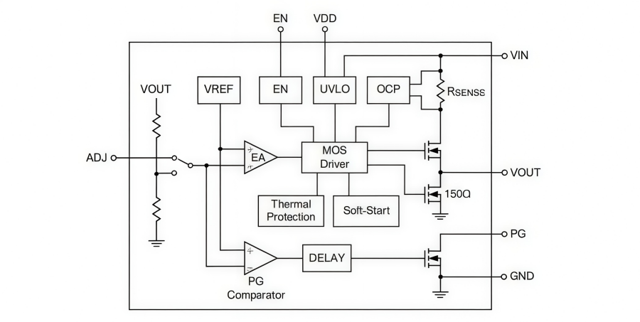
The diagram shows that the core of the RT9059GSP linear regulator consists of an error amplifier (EA), MOS driver, reference voltage (VREF), and soft-start circuit. The input voltage VIN is controlled by an internal MOSFET to produce the output VOUT. A current sense resistor (RSENSE) provides overcurrent protection (OCP). The ADJ pin sets the output voltage, the EN pin enables the chip, VDD powers the internal circuits, and the PG (Power-Good) signal indicates the output voltage status.
The chip also includes undervoltage lockout (UVLO), thermal protection, delay circuit (DELAY), and a PG comparator. These features ensure safe operation under input voltage faults, overcurrent, or overheating. The soft-start function prevents startup spikes, allows smooth output rise, and improves system reliability.
ANDE Electronics: Your Trusted Partner in Electronic Component Sourcing
At ANDE Electronics, we make getting the electronic components you need simple and fast. We work directly with top global manufacturers to provide high-quality components that have passed our strict checks, so you can count on them for your projects.
We also focus on quick and consistent delivery to keep your work on schedule and avoid delays. When you need reliable and efficient electronic parts for your projects, ANDE Electronics is a partner you can trust.


