Overview
The ST1S14PHR is a 3A step-down monolithic switching regulator designed for efficient DC/DC power conversion. It integrates a high-side N-channel DMOS transistor with a typical RDS(on) of 200mΩ, supporting a compact design with fewer external components. The output voltage is adjustable from 1.22V, with a fixed 850kHz switching frequency provided by the internal oscillator.
The device is available in an HSOP8 package with exposed frame, offering improved thermal performance for high-current applications. It also integrates a Power Good output, pulse-by-pulse current limit, short-circuit protection, and current foldback protection, making it suitable for industrial equipment, embedded systems, and other power management applications.
Basic Specifications
Parameter | Value |
Part Number | ST1S14PHR |
Description | IC REG BUCK ADJ 3A 8HSOP |
Manufacturer | STMicroelectronics |
Lead Free Status / RoHS Status | Lead free / RoHS Compliant |
Synchronous Rectifier | No |
Moisture Sensitivity Level (MSL) | 1 (Unlimited) |
Function | Step-Down |
Output Type | Adjustable |
Topology | Buck |
Number of Outputs | 1 |
Voltage - Input (Max) | 48V |
Voltage - Output (Max) | 43.2V |
Voltage - Output (Min/Fixed) | 1.22V |
Mounting Type | Surface Mount |
Voltage - Input (Min) | 5.5V |
Output Configuration | Positive |
Operating Temperature | -40°C ~ 125°C (TJ) |
Current - Output | 3A |
Package / Case | 8-SOIC |
Base Part Number | ST1S14 |
Pin Description

1. BOOT: Bootstrap capacitor for N-channel gate driver. Connects 100 nF low ESR capacitor from BOOT pin to SW
2. PG: Power good
3. EN1: Enable pin active low
4. FB: Feedback voltage
5. EN2: Enable pin active high
6. GND: Ground pin
7. VIN: Input supply pin
8. SW: Switching node
Key Features
l 3 A DC output current
l Operating input voltage from 5.5 V to 48 V
l 850 kHz internally fixed switching frequency
l Internal soft-start
l Power good open collector output
l Current mode architecture
l Embedded compensation network
l Zero load current operation
l Internal current limiting
l Inhibit for zero current consumption
l 2 mA maximum quiescent current over temperature range
l 250 mΩ typ. RDS(on)
l Thermal shutdown
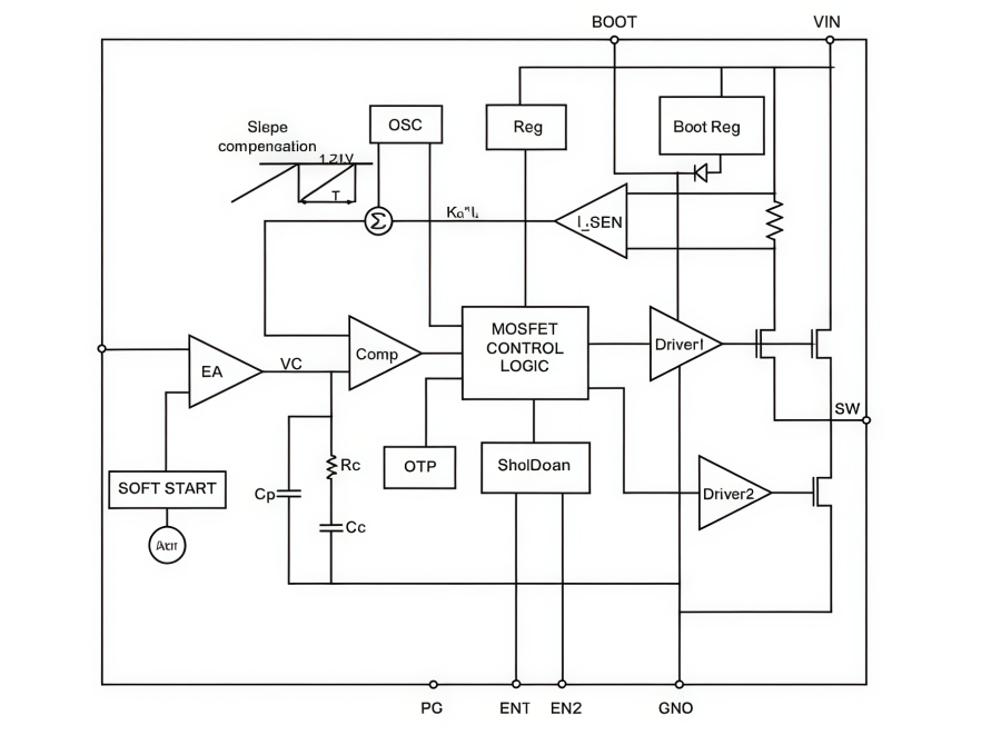
Functional Block Diagram Analysis
The ST1S14 is based on a “peak current mode”, constant frequency control. As a consequence, the intersection between the error amplifier output and the sensed inductor current generates the control signal to drive the power switch.
The main internal blocks shown in the block diagram are:
l A fully integrated sawtooth oscillator with a typical frequency of 850 kHz
l A transconductance error amplifier
l A high side current sense amplifier to track the inductor current
l A pulse width modulator (PWM) comparator and the circuitry necessary to drive the internal power element
l Soft-start circuitry to decrease the inrush current at power-up
l Current limitation circuit based on the pulse-by-pulse current protection with frequency divider based on FB voltage and the hiccup protection
l Bootstrap circuitry to drive the embedded N-MOS switch
l A multi input inhibit block for standby operation
l A circuit to implement the thermal protection function
Hardware Design & Topology
The ST1S14PHR uses an asynchronous Buck topology, where the high-side MOSFET and external Schottky diode work together to convert high input voltage into a stable output voltage. Proper selection of external components helps improve efficiency, reduce ripple, and ensure reliable operation.
1. Input Capacitor (CIN)
The input capacitor reduces switching noise and input voltage ripple.
l Use low ESR/ESL X5R or X7R MLCC capacitors.
l Recommended capacitance: 10μF–22μF, with a 100nF bypass capacitor placed close to VIN and GND pins.
l Voltage rating should be at least 1.5–2 times the maximum input voltage to avoid DC bias effects.
2. Schottky Diode (D1)
The external diode provides the current path when the MOSFET turns off.
l Reverse voltage rating should meet: VRRM ≥1.25×VIN,MAX
l Select low forward voltage (0.4–0.55V) Schottky diodes to reduce conduction loss and improve efficiency.
3. Power Inductor (L)
The inductor stores energy and controls output ripple current.
l Recommended ripple current ratio: 20–40% of output current.
l Saturation current should be higher than peak inductor current with 20–30% margin.
l Current rating should support the maximum continuous output current.
4. Feedback Resistors (R1/R2)
The feedback network controls output voltage regulation.
VOUT=1.22V×(1+R2/R1)
l Use 1% precision resistors for accurate voltage control.
l Recommended R2 range: 10kΩ–100kΩ.
5. Bootstrap Capacitor (CBOOT)
The bootstrap capacitor provides the gate drive voltage for the high-side N-MOSFET.
l Place a 100nF / 50V low-ESR X7R ceramic capacitor close to the BOOT and SW pins.
l Keep the connection short to reduce switching noise and improve stability.
Software Integration and Debug
1. Communication Interfaces and Control Modes
The device supports SPI, I²C, and MDIO/MDC interfaces for configuration and monitoring. SPI provides high-speed register access, I²C is used for low-speed control, and MDIO supports PHY status monitoring and IEEE 802.3 register access. Proper clock settings and reset timing are required before register initialization.
2. Embedded/Linux Driver Support
For Linux integration, the device is configured through the Device Tree, including bus address, compatible settings, PHY mode, speed, and MAC mapping. The Linux DSA framework is commonly used to manage each switch port as an independent network interface.
3. Debugging and Fault Diagnosis
System debugging relies on status registers, MIB counters, and loopback functions. Link status, auto-negotiation errors, CRC errors, and packet loss can be monitored for troubleshooting. Fault flags such as over-temperature and UVLO help improve system reliability.
Typical Application Scenarios
The ST1S14PHR is a high-current step-down switching regulator capable of delivering up to 3A output current, making it suitable for applications that require efficient power conversion, stable voltage regulation, and compact power solutions.
1. Factory Automation Equipment
ST1S14PHR is suitable for industrial automation systems that require stable power supplies for controllers, sensors, and communication modules. Its high-current capability and protection functions help maintain reliable operation in continuous industrial environments.
2. Printers and Office Equipment
The regulator can provide efficient DC power conversion for printers and multifunction devices, supporting motors, control circuits, and electronic modules that require stable voltage rails. Its compact design helps reduce the size of power management circuits.
3. DC-DC Power Modules
With adjustable output voltage starting from 1.22V and an integrated high-side MOSFET, ST1S14PHR can be used as a core component in compact DC-DC converter modules. It simplifies circuit design while providing high conversion efficiency for various voltage regulation needs.
4. High-Current LED Driver Applications
The device can support LED lighting systems that require stable current delivery and efficient voltage conversion. Its high output capability and thermal performance make it suitable for driving high-power LED loads in industrial and commercial lighting applications.
5. Embedded Systems and Control Boards
ST1S14PHR provides a reliable power solution for embedded systems that integrate processors, communication chips, and peripheral devices. Its small package size and integrated protection features help improve system reliability while reducing external components.
How Does ST1S14PHR Work as a Buck Converter?
The ST1S14PHR operates as an asynchronous buck converter, using an internal high-side N-channel DMOS switching transistor together with an external freewheeling diode to convert a higher input voltage into a stable lower output voltage. When the internal switch is turned on, energy is delivered from the input source to the load through the inductor while the inductor stores energy. When the switch turns off, the inductor releases stored energy through the external diode, maintaining continuous current flow and achieving smooth voltage step-down conversion.
The device integrates a fixed 850kHz oscillator and uses PWM control to adjust the switching duty cycle, ensuring stable output regulation. The feedback pin continuously monitors the output voltage and adjusts the switching operation according to the set value. In addition, the ST1S14PHR features cycle-by-cycle current limiting, short-circuit protection, and current foldback protection, helping reduce power stress under abnormal conditions and improve overall system reliability.
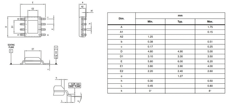
Package Dimensions
ANDE Electronics: Your Trusted Partner in Electronic Component Sourcing
At ANDE Electronics, we make getting the electronic components you need simple and fast. We work directly with top global manufacturers to provide high-quality components that have passed our strict checks, so you can count on them for your projects.
We also focus on quick and consistent delivery to keep your work on schedule and avoid delays. When you need reliable and efficient electronic parts for your projects, ANDE Electronics is a partner you can trust.